Engineers just created a “phonon laser” that could shrink your next smartphone
- Date:
- January 17, 2026
- Source:
- University of Colorado at Boulder
- Summary:
- Engineers have created a device that generates incredibly tiny, earthquake-like vibrations on a microchip—and it could transform future electronics. Using a new kind of “phonon laser,” the team can produce ultra-fast surface waves that already play a hidden role in smartphones, GPS systems, and wireless tech. Unlike today’s bulky setups, this single-chip device could deliver far higher performance using less power, opening the door to smaller, faster, and more efficient phones and wireless devices.
- Share:
Engineers have taken a major step toward producing the smallest earthquakes ever created, shrinking seismic-style vibrations down to the scale of a microchip.
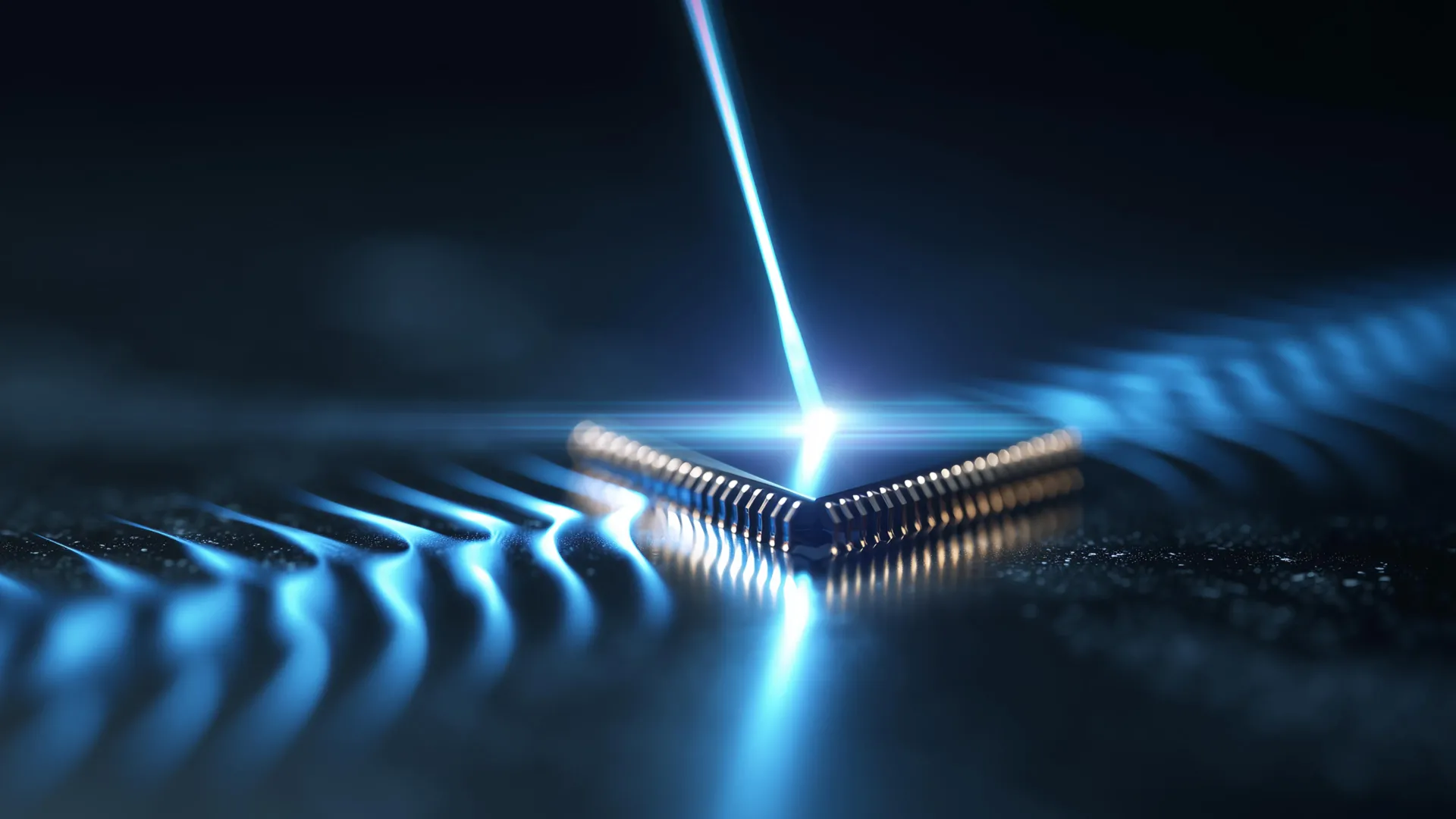
The breakthrough centers on a device called a surface acoustic wave phonon laser. The technology could eventually enable more advanced chips for smartphones and other wireless electronics, helping make them smaller, faster, and more energy efficient.
The research was led by Matt Eichenfield, an incoming faculty member at the University of Colorado Boulder, along with scientists from the University of Arizona and Sandia National Laboratories. Their findings were published Jan. 14 in the journal Nature.
What Are Surface Acoustic Waves?
The new device relies on surface acoustic waves, commonly known as SAWs. These waves behave somewhat like sound waves, but instead of traveling through the air or deep inside a material, they move only along its surface.
Large earthquakes naturally produce powerful surface acoustic waves that ripple across the Earth's crust, shaking buildings and causing damage. On a much smaller scale, SAWs are already essential to modern technology.
"SAWs devices are critical to the many of the world's most important technologies," said Eichenfield, senior author of the new study and Gustafson Endowed Chair in Quantum Engineering at CU Boulder. "They're in all modern cell phones, key fobs, garage door openers, most GPS receivers, many radar systems and more."
How SAWs Already Power Smartphones
Inside a smartphone, SAWs function as highly precise filters. Radio signals arriving from a cell tower are first converted into tiny mechanical vibrations. This allows chips to separate useful signals from interference and background noise. The cleaned vibrations are then converted back into radio waves.
In this study, Eichenfield and his colleagues introduced a new way to generate these surface waves using what they call a phonon laser. Unlike a typical laser pointer that emits light, this device produces controlled vibrations.
"Think of it almost like the waves from an earthquake, only on the surface of a small chip," said Alexander Wendt, a graduate student at the University of Arizona and lead author of the study.
Most existing SAW systems require two separate chips and an external power source. The new design combines everything into a single chip and could operate using just a battery while reaching much higher frequencies.
A Laser Built for Vibrations
To understand the new device, it helps to start with how conventional lasers work.
Many everyday lasers are diode lasers, which create light by bouncing it between two tiny mirrors on a semiconductor chip. As the light reflects back and forth, it interacts with atoms energized by an electric current. Those atoms release additional light, strengthening the beam.
"Diode lasers are the cornerstone of most optical technologies because they can be operated with just a battery or simple voltage source, rather than needing more light to create the laser like a lot of previous kinds of lasers," Eichenfield said. "We wanted to make an analog of that kind of laser but for SAWs."
To achieve this, the team built a bar-shaped device about half a millimeter long.
A Stack of Specialized Materials
The device consists of several layered materials. At its base is silicon, the same material used in most computer chips. Above that sits a thin layer of lithium niobate, a piezoelectric material. When lithium niobate vibrates, it produces oscillating electric fields, and those electric fields can also trigger vibrations.
The final layer is an extremely thin sheet of indium gallium arsenide. This material has unusual electronic properties and can accelerate electrons to very high speeds even under weak electric fields.
Together, these layers allow vibrations traveling along the lithium niobate surface to interact directly with fast-moving electrons in the indium gallium arsenide.
Making Waves Build Like a Laser
The researchers describe the device as working similarly to a wave pool.
When electric current flows through the indium gallium arsenide, surface waves form in the lithium niobate layer. These waves travel forward, strike a reflector, and then move backward, much like light reflecting between mirrors in a laser. Each forward pass strengthens the wave, while each backward pass weakens it.
"It loses almost 99% of its power when it's moving backward, so we designed it to get a substantial amount of gain moving forward to beat that," Wendt said.
After repeated passes, the vibrations grow strong enough that a portion escapes from one side of the device, similar to how laser light eventually exits its cavity.
Faster Waves, Smaller Devices
Using this approach, the team generated surface acoustic waves vibrating at about 1 gigahertz, meaning billions of oscillations per second. The researchers believe the same design could be pushed into tens or even hundreds of gigahertz.
Traditional SAW devices typically max out at around 4 gigahertz, making the new system far faster.
Eichenfield said the advance could lead to wireless devices that are smaller, more powerful, and more energy efficient.
In today's smartphones, multiple chips repeatedly convert radio waves into SAWs and back again whenever users send messages, make calls, or browse the internet. The researchers aim to simplify that process by creating a single chip that handles all of the signal processing using surface acoustic waves.
"This phonon laser was the last domino standing that we needed to knock down," Eichenfield said. "Now we can literally make every component that you need for a radio on one chip using the same kind of technology."
Story Source:
Materials provided by University of Colorado at Boulder. Note: Content may be edited for style and length.
Journal Reference:
- Alexander Wendt, Matthew J. Storey, Michael Miller, Dalton Anderson, Eric Chatterjee, William Horrocks, Brandon Smith, Ping-Show Wong, Shawn Arterburn, Thomas A. Friedmann, Lisa Hackett, Matt Eichenfield. An electrically injected solid-state surface acoustic wave phonon laser. Nature, 2026; 649 (8097): 597 DOI: 10.1038/s41586-025-09950-8
Cite This Page: