Scientists finally see the atomic flaws hiding inside computer chips
- Date:
- March 5, 2026
- Source:
- Cornell University
- Summary:
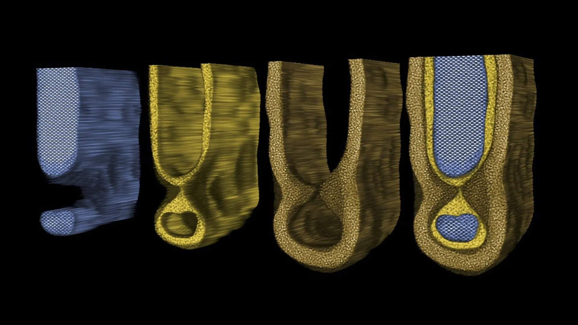
- Researchers at Cornell University have developed a powerful imaging technique that reveals atomic scale defects inside computer chips for the first time. Using an advanced electron microscopy method, the team mapped the exact positions of atoms inside tiny transistor structures and uncovered small imperfections nicknamed “mouse bites.” These defects form during the complex manufacturing process and can disrupt how electrons flow through a chip’s channels, which are only about 15 to 18 atoms wide.
- Share:
Researchers at Cornell University have used high resolution 3D imaging to identify atomic scale defects inside computer chips for the first time. These tiny imperfections can interfere with chip performance, making them a major concern for modern electronics.
The new imaging technique was developed through a collaboration with Taiwan Semiconductor Manufacturing Company (TSMC) and Advanced Semiconductor Materials (ASM). Because computer chips power devices ranging from smartphones and cars to AI data centers and quantum computers, the discovery could influence many areas of technology.
The findings were published Feb. 23 in Nature Communications. Doctoral student Shake Karapetyan served as the study's lead author.
"Since there's really no other way you can see the atomic structure of these defects, this is going to be a really important characterization tool for debugging and fault-finding in computer chips, especially at the development stage," said David Muller, the Samuel B. Eckert Professor of Engineering in the Cornell Duffield College of Engineering, who led the project.
Why Tiny Defects Matter in Semiconductor Chips
Extremely small structural flaws have long challenged the semiconductor industry. As chips have grown more complex and their components have shrunk to the scale of individual atoms, even minor irregularities can affect how devices operate.
At the center of every computer chip is the transistor. This tiny component acts as a switch that controls the movement of electrical current. Each transistor contains a channel that opens and closes to regulate the flow of electrons.
"The transistor is like a little pipe for electrons instead of water," Muller said. "You can imagine, if the walls of the pipe are very rough, it's going to slow things down. And so measuring how rough the walls are and which walls are good and which walls are bad is now even more important."
From Early Transistors to 3D Chip Structures
Muller has long studied the physical limits of semiconductor technology. From 1997 to 2003 he worked in the research and development division of Bell Labs -- where transistors were invented -- investigating how small these devices could ultimately become.
When transistors first appeared in the mid 20th century, they were arranged across chips in flat layouts that spread outward, similar to suburbs expanding across land. Over time engineers ran out of surface area, which led them to begin stacking transistors vertically, creating complex three dimensional structures that resemble high rise apartment buildings.
"The problem is these 3D structures are smaller than the size of a virus. And these days, it's a lot smaller. It's more like a molecule-in-the-cell kind of scale," Muller said.
Today a single advanced chip can contain billions of transistors. As their size has continued to shrink, diagnosing performance issues has become far more difficult.
"These days, a transistor channel can be only about 15 to 18 atoms wide, which is super, super tiny, and they're extremely intricate," Karapetyan said. "At this point, it matters where every atom is, and it's really hard to characterize."
Advances in Electron Microscopy
Earlier in his career at Bell Labs, Muller worked with fellow scientist Glen Wilk '90, who is now vice president of technology at ASM. The pair studied ways to replace silicon dioxide, the dominant gate material at the time, which leaked too much current when devices became very small. Their research helped advance the use of hafnium oxide, which later became the standard material used in computer processors and mobile devices beginning in the mid-aughts.
"The papers we published on how to use electron microscopes to characterize these materials, I can tell you, a lot of the semiconductor folks had read those very, very carefully," said Muller, who co-directs the Kavli Institute at Cornell for Nanoscale Science and the Cornell Center for Materials Research (CCMR). "When we got back into this project, that was very clear. And the microscopy has gone a very long way. Back then, it was like flying biplanes. And now you've got jets."
The "jet" Muller refers to is electron ptychography. This computational imaging technique relies on an electron microscope pixel array detector (EMPAD), a technology co-developed by Muller's research group. The detector records detailed patterns created as electrons pass through the transistor structures.
By comparing how these scattering patterns shift from one scan point to another, researchers can reconstruct extremely detailed images. The system is so precise that it has produced the highest resolution images ever captured, allowing scientists to see individual atoms with extraordinary clarity, a capability recognized by Guinness World Records.
Discovering "Mouse Bite" Defects
More than 25 years after their earlier collaboration, Muller and Wilk worked together again with support from TSMC and its Corporate Analytical Laboratories group. Their goal was to apply the EMPAD technology to modern semiconductor devices.
"You can think of this imaging technique like solving a massive puzzle, both in terms of taking the experimental data and doing the computational reconstruction," Karapetyan said.
After collecting and reconstructing the imaging data, the researchers tracked the positions of atoms within the transistor channels. This analysis revealed subtle roughness at the interfaces of these channels. Karapetyan described these irregular patterns as "mouse bites."
The defects formed during the optimized growth process used to manufacture the structures. Sample devices created at the nanoelectronics research center Imec provided an ideal platform for testing the imaging technique.
"Fabrication of modern devices takes hundreds, if not thousands, of steps of chemical etching and deposition and heating, and then every single step does something to your structure," Karapetyan said. "Before you used to look at projective images to try to figure out what was really going on. Now you have a direct probe to actually see after every single step and have a better grasp of, oh, I put the temperature this high, and then this is what it looks like."
Implications for Future Chips and Quantum Computing
The ability to directly observe atomic level defects could influence nearly every device that relies on advanced computer chips, including smartphones, laptops, and large data centers. It may also help researchers develop emerging technologies such as quantum computers, which require extremely precise control over the structure of materials.
"I think there's a lot more science we can do now, and a lot more engineering control, having this tool," Karapetyan said.
Co-authors of the study include Steven Zeltmann, staff scientist at Platform for the Accelerated Realization, Analysis and Discovery of Interface Materials (PARADIM), along with Ta-Kun Chen and Vincent Hou of TSMC.
The research was funded by TSMC. Support for the microscopy facilities was provided by CCMR and PARADIM, which are funded by the National Science Foundation.
Story Source:
Materials provided by Cornell University. Note: Content may be edited for style and length.
Journal Reference:
- Shake Karapetyan, Steven E. Zeltmann, Glen Wilk, Ta-Kun Chen, Vincent D.-H. Hou, David A. Muller. 3D atomic-scale metrology of strain relaxation and roughness in Gate-All-Around transistors via electron ptychography. Nature Communications, 2026; DOI: 10.1038/s41467-026-69733-1
Cite This Page: